









According to Fast Technology on May 26, Huawei’s newly announced “Tao (τ) Law” has sent shockwaves through the semiconductor industry and attracted significant attention from overseas media.
Tom’s Hardware reported that Huawei’s next-generation flagship smartphone series, the Mate 90, will become one of the first commercial smartphones powered by processors built on the new LogicFolding architecture.
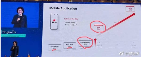
At the IEEE International Symposium on Circuits and Systems (ISCAS 2026) held in Shanghai on May 25, He Tingbo, Huawei board member and President of HiSilicon Semiconductor, officially unveiled the “Tao Law” along with Huawei’s self-developed LogicFolding technology architecture during a keynote speech.
She revealed that Huawei has spent six years secretly developing the technology and has already designed and mass-produced 381 chips based on the concept, serving a wide range of industries.
Moving Beyond Moore’s Law
As is well known, the traditional semiconductor industry follows Moore’s Law, improving chip performance by continuously shrinking transistor sizes. However, this path relies heavily on advanced Western equipment such as EUV lithography machines.
Under ongoing U.S. sanctions, HiSilicon has taken a different approach by proposing the Tao Law, which replaces “geometric scaling” with “time scaling.” Instead of focusing solely on miniaturization, the new method prioritizes optimizing signal transmission speed within the system.
LogicFolding Architecture Explained
As the commercial implementation of Tao Law, the LogicFolding architecture physically folds and stacks logic circuits into a dual-layer structure. This significantly shortens internal chip wiring distances and reduces signal latency.
The approach allows Huawei to create processors comparable to world-leading chips without depending on Western advanced manufacturing equipment.
Kirin 2026 Delivers Surprising Results
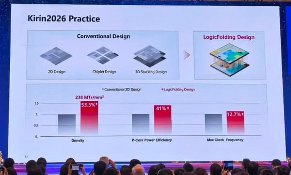
The Kirin 2026 chip (a codename expected to eventually launch as the Kirin 9050 Pro) is the first successful implementation of LogicFolding technology and has reportedly delivered results far beyond expectations.
Testing shows that compared with the Kirin 9030 Pro:
- Transistor density increased by 53.5%
- Density reached 238 MTr/mm² (million transistors per square millimeter)
- This level is theoretically comparable to Intel’s 18A process
- It is also close to first-generation TSMC 3nm technology
At the same time:
- Performance-core power efficiency improved by 41%
- Maximum clock frequency increased by 12.7%
These results represent a major leap in both performance and energy efficiency.
SMIC Manufacturing and Performance Claims
Notably, CITIC Construction Investment analyst Yu Fangbo previously revealed that the Kirin 9050 chip planned for the Huawei Mate 90 series would be manufactured by SMIC using this innovative logic-stacking approach.
Despite relying only on DUV-level lithography machines, the chip’s testing results reportedly exceeded expectations. According to the report, its performance surpasses Apple’s A18 chip released in 2024 and is comparable to chips produced using TSMC’s 3nm process.
Huawei’s Long-Term Semiconductor Plans
According to Huawei’s roadmap, the LogicFolding architecture will first be used in flagship smartphone processors before expanding into Ascend AI processors and large-scale data center clusters.
The technology is expected to provide domestic alternatives to restricted NVIDIA products in the Chinese market.
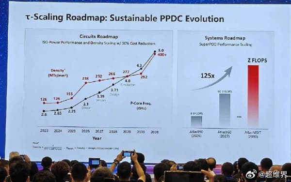
By 2031, Huawei hopes to design high-end chips with transistor density equivalent to a 1.4nm process, potentially giving a major boost to China’s semiconductor self-sufficiency efforts.